Surface-mount technology (SMT) is a method for making electronic circuits in which the components are mounted or placed directly onto the surface of printed circuit boards (PCBs). An electronic device so made is called a surface-mount device (SMD).
Description
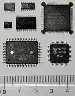
An SMT component is usually smaller than its through-hole counterpart because it has either smaller leads or no leads at all. It may have short pins or leads of various styles, flat contacts, a matrix of solder balls (BGAs), or terminations on the body of the component. Components were mechanically redesigned to have small metal tabs or end caps that could be directly soldered to the surface of the PCB. Components became much smaller and component placement on both sides of a board became far more common with surface mounting than through-hole mounting, allowing much higher circuit densities.
An SMT component is usually smaller than its through-hole counterpart because it has either smaller leads or no leads at all. It may have short pins or leads of various styles, flat contacts, a matrix of solder balls (BGAs), or terminations on the body of the component.Surface mounting was originally called “planar mounting”. Surface-mount technology was developed in the 1960s and became widely used in the late 1980s.
Much of the pioneering work in this technology was by IBM. The design approach first demonstrated by IBM in 1960 in a small-scale computer was later applied in the Launch Vehicle Digital Computer used in the Instrument Unit that guided all Saturn IB and Saturn V vehicles. Components were mechanically redesigned to have small metal tabs or end caps that could be directly soldered to the surface of the PCB.
Components became much smaller and component placement on both sides of a board became far more common with surface mounting than through-hole mounting, allowing much higher circuit densities. Often only the solder joints hold the parts to the board, although parts on the bottom or “second” side of the board may be secured with a dot of adhesive to keep components from dropping off inside reflow ovens if the part has a large size or weight. Adhesive is also used to hold SMT components on the bottom side of a board if a wave soldering process is used to solder both SMT and through-hole components simultaneously.
Alternatively, SMT and throughhole components can be soldered together without adhesive if the SMT parts are first reflow-soldered, then a selective solder mask is used to prevent the solder holding the parts in place from reflowing and the parts floating away during wave soldering. Surface mounting lends itself well to a high degree of automation, reducing labor cost and greatly increasing production rates. SMDs can be onequarter to one-tenth the size and weight, and one-half to one-quarter the cost of equivalent through-hole parts.
Also Read : Hydrogen Super Highway
Advantages of SMT
The main advantages of SMT over the older through-hole technique are:
Σ Smallest package of SMT is 0402 (0.25 × 0.125 mm).
Σ Smaller components. As of 2012 smallest was 0.4 × 0.2 mm (0.016 in × 0.008 in: 01005).
Σ Much higher component density (components per unit area) and many more connections per component.
Σ Lower initial cost and time of setting up for production.
Σ Fewer holes need to be drilled.
Σ Simpler and faster automated assembly. Some placement machines are capable of placing more than 136,000 components per hour.
Σ Small errors in component placement are corrected automatically as the surface tension of molten solder pulls components into alignment with solder pads.
Σ Components can be placed on both sides of the circuit board.
Σ Lower resistance and inductance at the connection; consequently, fewer unwanted RF signal effects and better and more predictable high-frequency performance.
Σ Better mechanical performance under shake and vibration conditions.
Σ Many SMT parts cost less than equivalent through-hole parts.
Σ Better EMC compatibility (lower radiated emissions) due to the smaller radiation loop area (because of the smaller package) and the smaller lead inductance.
Disadvantages of SMT
Σ Manual prototype assembly or component-level repair is more difficult and requires skilled operators and more expensive tools, due to the small sizes and lead spacings of many SMDs.
Σ SMDs cannot be used directly with plug-in breadboards (a quick snap-andplay prototyping tool), requiring either a custom PCB for every prototype or the mounting of the SMD upon a pin-leaded carrier. For prototyping around a specific SMD component, a less-expensive breakout board may be used. Additionally, stripboard style protoboards can be used, some of which include pads for standard sized SMD comportments. For prototyping, “dead bug” breadboarding can be used.
Σ SMDs’ solder connections may be damaged by potting compounds going through thermal cycling.
Σ Solder joint dimensions in SMT quickly become much smaller as advances are made toward ultra-fine pitch technology. The reliability of solder joints becomes more of a concern, as less and less solder is allowed for each joint. Voiding is a fault commonly associated with solder joints, especially when reflowing a solder paste in the SMT application. The presence of voids can deteriorate the joint strength and eventually lead to joint failure.
Σ SMT is unsuitable for large, high-power, or high-voltage parts, for example in power circuitry. It is common to combine SMT and through-hole construction, with transformers, heat-sinked power semiconductors, physically large capacitors, fuses, connectors, and so on mounted on one side of the PCB through holes.
Σ SMT is unsuitable as the sole attachment method for components that are subject to frequent mechanical stress, such as connectors that are used to interface with external devices that are frequently attached and detached.
Assembly Work
Where components are to be placed, the printed circuit board normally has flat, usually tin-lead, silver, or gold plated copper pads without holes, called solder pads. Solder paste, a sticky mixture of flux and tiny solder particles, is first applied to all the solder pads with a stainless steel or nickel stencil using a screen printing process. It can also be applied by a jet-printing mechanism, similar to aninkjet printer. After pasting, the boards then proceed to the pick-and-place machines, where they are placed on a conveyor belt. The components to be placed on the boards are usually delivered to the production line in either paper/plastic tapes wound on reels or plastic tubes. Some large integrated circuits are delivered in static-free trays.
Numerical control pick-and-place machines remove the parts from the tapes, tubes or trays and place them on the PCB. The boards are then conveyed into the reflow soldering oven. They first enter a pre-heat zone, where the temperature of the board and all the components is gradually, uniformly raised. The boards then enter a zone where the temperature is high enough to melt the solder particles in the solder paste, bonding the component leads to the pads on the circuit board. The surface tension of the molten solder helps keep the components in place, and if the solder pad geometries are correctly designed, surface tension automatically aligns the components on their pads. There are a number of techniques for reflowing solder.
References
1. Wikipedia.org
2. Surface Mount Status
3. Cornell Dubilier, Application Guide – Aluminium SMT Capacitors
4.”High-resolution photos of components/PCBs”. Spaceaholic.com. Retrieved 2011-07-07.
5. “Surface mount technology status”
6. “High-resolution photos of components/PCBs”. Spaceaholic.com.


Pingback: E-Paper Technology | Seminar Topic for CSE Students - Seminarsonly.com