


Published on Feb 14, 2025
During the last two decades, there has been an exponential growth in the operational speed of microprocessors. Also RAM capacities have been improving at more than fifty percent per year. However the speed and access time of the memory have been improving at slower rate. In order to keep up in performance and reliability with processor technology it is necessary to make considerable improvements in the memory access time.
The Rambus founders emerged with a memory technology-RD RAM. RDRAM memory provides the highest bandwidth -2.1GB/sec. per pin- from the fewest pins at five-times the speed of industry available DRAM. The RDRAM memory channel achieves its high-speed operation through several innovative techniques including separate control and address buses, highly efficient protocol, low voltage signaling, and precise clocking to minimize skew between clock and data lines. A single RDRAM device is capable of transferring data at 1066Mb/sec. per-pin to Rambus-compatible ICs. Data rate per-pin will increase beyond 1066Mb/sec per pin in the future.
Currently, there are three major groups of memory technology widely available in the market: Synchronous DRAM (SDRAM), Double Data Rate Synchronous DRAM (DDR SDRAM) and RDRAM memory. SDRAM and DDR SDRAM share many architectural and signaling features. Both use a parallel data bus, mainly available in component widths of x8 or x16, both have a single addressing command bus that must be shared to transmit row and column addresses.
DDR SDRAM increases data bandwidth over conventional SDRAM by transmitting data on both edges of the synchronous clock signal using SSTL-2 signaling, thus in theory “doubling” the data rate of the memory. It, However does not double the address command bandwidth of the system by using both the edges of the clock on the command bus, a factor that ultimately limits the performance from using DDR signaling on the data bus.
RDRAM memory takes a totally different approach. It combines a conventional DRAM core with a high-speed serial interface called the RDRAM channel. The Channel uses 16 pins ( 2 bytes) for a data path operating at an effective data rate of 800 MHz per pin by transmitting data on both edges of the clock. To facilitate maximum performance, the RDRAM channel utilizes double data rate signaling on non-multiplexed row and column address command buses.
Since each RDRAM device’s data path is as wide as the Channel, a single device can service an entire memory request, unlike SDRAM, which uses multiple devices in parallel to satisfy a request. Up to 32 RDRAM devices can be placed on each Channel without a buffer. The Channel is common to all devices and incorporates the command bus, data bus and a serial control bus for initialization. The RDRAM Channel is uniformly loaded as new devices are added. The RDRAM protocol supports many features that optimize the bandwidth and efficiency of the overall system.
A brief overview of the Rambus (RDRAM) memory subsystem and comparing it to SDRAM PC133 gives the following information. The maximum theoretical data bandwidth of SDRAM (PC133 specification) is 1064 Mbytes/sec. This is calculated from 64 data lines (8 bytes) working at 133 MHz. In practice this theoretical maximum, or peak, throughout can be sustained for only short bursts of time. For extended data transfers only 65 percent of this value (around 692 MBytes/sec) can be maintained. The 800 MHz Rambus channel offers a theoretical and practical maximum bandwidth of 1600 MBytes/sec per channel.
The following diagrams compare the different data bandwidths within the PC using an Intel Pentium® III 800 MHz processor, and a 133 MHz system bus:
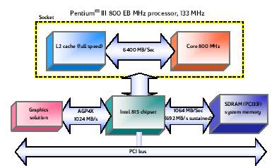
:Comparison of data bandwidths for PC systems with SDRAM and Rambus memory
As can be seen, the memory data bandwidth is similar to that of the graphics bandwidth which helps to ‘balance’ out the different data channels (between processor, chipset, memory, and graphics subsystem) and ensure that no single bus creates a bottleneck. The result is a better overall system performance.
| Are you interested in this topic.Then mail to us immediately to get the full report.
email :- contactv2@gmail.com |
